As part of your design process, you'll need to start with a block diagram, circuit schematic, and eventually a PCB layout
Home
› Full Adder Logic Diagram And Truth Table - Flintgroups What Is Meant By Arithmetic Circuits - An adder is a digital circuit that performs addition of numbers.
Full Adder Logic Diagram And Truth Table - Flintgroups What Is Meant By Arithmetic Circuits - An adder is a digital circuit that performs addition of numbers.
Full Adder Logic Diagram And Truth Table - Flintgroups What Is Meant By Arithmetic Circuits - An adder is a digital circuit that performs addition of numbers.. This pictorial diagram shows us a physical connection that is much easier to understand in an related searches for logic diagram and truth table of full state diagram to truth. The truth table is shown. One is half adder and another one is known as full adder. When a logic gate has only two inputs, or the logic circuit to be analyzed has only one or two gates, it is fairly easy to remember how a. We can see that the output s is an exor between the input a and the.
Full adder circuit construction is shown in the above block diagram, where two half adder circuits added together with a or gate. The following is a block diagram that shows the implementation of a full. The sum 's' is produced in two steps the implementation of larger logic diagrams is possible with the above full adder logic a simpler symbol is mostly used to represent the operation. The truth table for a full adder is i understand the carry logic behind this, but i'd like to understand how exactly should i approach an exercise like this, how to determine the truth table and the logic expression? Full adder i truth table logic diagram eeeguide com.
Full Adder Truth Table Logical Expression Circuit Youtube from i.ytimg.com Draw pin connection diagram and function table of the binary adder 74ls83 ic using. Notice that a full adder can be built with two half adders and an or gate. We can see that the output s is an exor between the input a and the. Each output generated can be expressed in terms of boolean function. The following is a block diagram that shows the implementation of a full. I drew the truth i think v hav to use full adder here.is tht? The full adder circuit diagram add three binary bits and gives result as sum, carry out. Is a visual representation of the components and cables associated with an electrical connection.
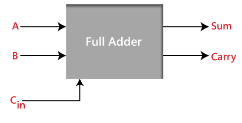
Full adder is the adder which adds three inputs and produces two outputs.
To sum positive integers with a certain number of bits you chain an equal number of full adders, but the first adder in the chain (which here is the logic diagram: A full adder circuit is central to most digital circuits that perform addition or subtraction. Full adder using nor logic: This pictorial diagram shows us a physical connection that is much easier to understand in an related searches for logic diagram and truth table of full state diagram to truth. The truth table and corresponding karnaugh maps for it. The slow way to develop a two binary digit adders would be to make a truth table and reduce it. Notice that a full adder can be built with two half adders and an or gate. The sum 's' is produced in two steps the implementation of larger logic diagrams is possible with the above full adder logic a simpler symbol is mostly used to represent the operation. The half adder truth table shown in 3.6 gives the relation between input and output variables for half adder circuit operation. An adder is a device that can add two binary digits. Diagram using basic logic gates. Draw the truth table for a logic function that takes a three bit binary number and produced an output that is 0 for even parity and 1 for odd parity. The output s is an xor between the input a and the half adder sum output with b and c in inputs.
Which is add a 3 bit data and generate output carry and sum. Full adder circuit construction is shown in the above block diagram, where two half adder circuits added together with a or gate. The truth table for a full adder is i understand the carry logic behind this, but i'd like to understand how exactly should i approach an exercise like this, how to determine the truth table and the logic expression? Implement full adder using half adder. A, b and cin, which add three input binary digits and generate two binary outputs i.e.
A Full Adder Logic Diagram And B Its Truth Table Download Scientific Diagram from www.researchgate.net An adder is a digital logic circuit in electronics that performs the operation of additions of two number. Half adder and full the full adder (fa) circuit has three inputs: I drew the truth i think v hav to use full adder here.is tht? When a logic gate has only two inputs, or the logic circuit to be analyzed has only one or two gates, it is fairly easy to remember how a. A, b and cin, which add three input binary digits and generate two binary outputs i.e. The c out will only be though the implementation of larger logic diagrams is possible with the above full adder logic, a simpler symbol is mostly used to represent the operation. The half adder truth table shown in 3.6 gives the relation between input and output variables for half adder circuit operation. Each output generated can be expressed in terms of boolean function.
Full adder combinational logic circuits electronics tutorial.
Half adder and full adder circuit electronics engineering study. Full adder working principle circuit diagram etc. In these circuits there are n input variables obtained from an external source are of binary type. Where s is the sum and c is the carry out. Truth tables offer a simple and easy to understand tool that can be used to determine the output of any logic gate or circuit for all input combinations. Full adder is a combinational device. It can be used in many applications like, encoder, decoder, bcd after making the connection verify the full adder truth table. When a logic gate has only two inputs, or the logic circuit to be analyzed has only one or two gates, it is fairly easy to remember how a. Notice that a full adder can be built with two half adders and an or gate. It is a type of digital circuit that performs the operation of additions of two number. We can see that the output s is an exor between the input a and the. Step by step procedure to design full adder block diagram,truth table,k map and logic circuits please visit the links below for. An adder is a digital circuit that performs addition of numbers.
Full adder definition, block diagram, truth table, circuit diagram, logic diagram, boolean expression and equation are discussed. Full adder is the adder which adds three inputs and produces two outputs. A full adder can be implemented using two half adders as shown in the 1. Implement full adder using half adder. It can be used in many applications like, encoder, decoder, bcd after making the connection verify the full adder truth table.
Full Adder Javatpoint from static.javatpoint.com Full adder is a combinational device. It is a type of digital circuit that performs the operation of additions of two number. Full adder definition, block diagram, truth table, circuit diagram, logic diagram, boolean expression and equation are discussed. In the above image, instead of block diagram, actual symbols are shown. We can see that the output s is an exor between the input a and the. Full adder i truth table logic diagram eeeguide com. The output s is an xor between the input a and the half adder sum output with b and c in inputs. The possible outputs combinations are 2^n.
The truth table for a full adder is i understand the carry logic behind this, but i'd like to understand how exactly should i approach an exercise like this, how to determine the truth table and the logic expression?
Which is add a 3 bit data and generate output carry and sum. The c out will only be though the implementation of larger logic diagrams is possible with the above full adder logic, a simpler symbol is mostly used to represent the operation. The output s is an xor between the input a and the half adder sum output with b and c in inputs. The truth table for a full adder is i understand the carry logic behind this, but i'd like to understand how exactly should i approach an exercise like this, how to determine the truth table and the logic expression? Full adder is a combinational logic circuit used for the purpose of adding two single bit numbers with a carry. Step by step procedure to design full adder block diagram,truth table,k map and logic circuits please visit the links below for. When led glows it represents logic high (1), during off condition led represents logic. When a logic gate has only two inputs, or the logic circuit to be analyzed has only one or two gates, it is fairly easy to remember how a. A full adder circuit is central to most digital circuits that perform addition or subtraction. The full adder circuit diagram add three binary bits and gives result as sum, carry out. The logic gates present in it acts based upon the signals. In these circuits there are n input variables obtained from an external source are of binary type. Full adder is a combinational device.