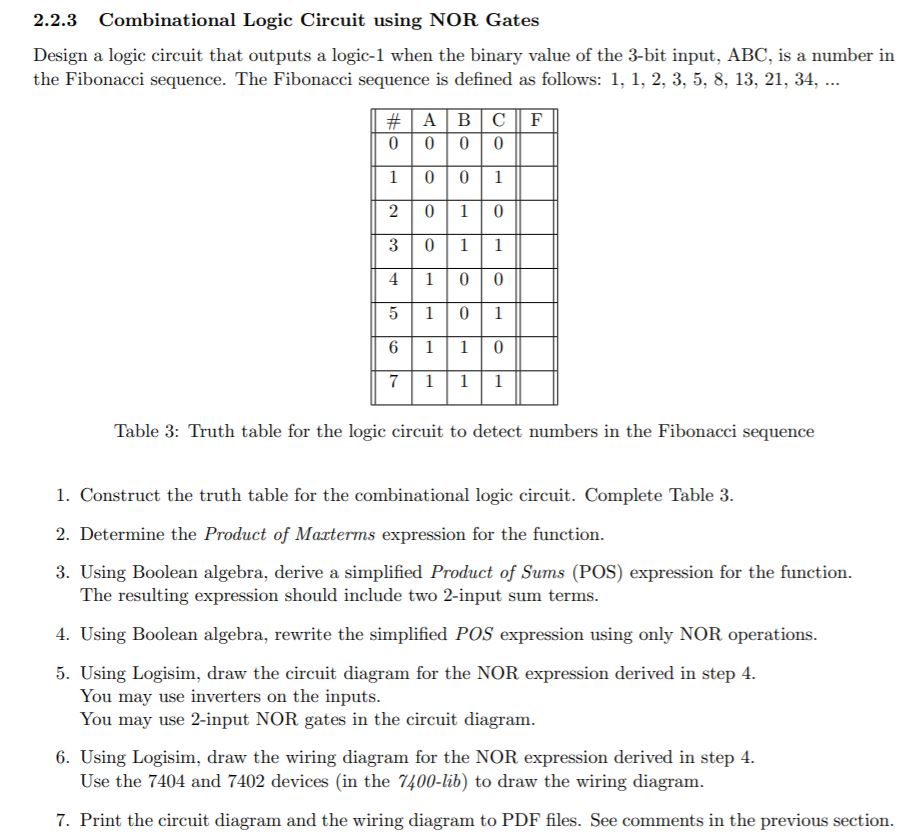
As part of your design process, you'll need to start with a block diagram, circuit schematic, and eventually a PCB layout
Home
› Logic Circuit Diagram Of 1 To 8 / Solved 3 Digital Logic Circuits 30 Points 10 Each A Chegg Com : Demultiplexer has one data input di and three select inputs s0, s1 and s3 and 8 outputs q0.0 to q0.7.;
Logic Circuit Diagram Of 1 To 8 / Solved 3 Digital Logic Circuits 30 Points 10 Each A Chegg Com : Demultiplexer has one data input di and three select inputs s0, s1 and s3 and 8 outputs q0.0 to q0.7.;
Logic Circuit Diagram Of 1 To 8 / Solved 3 Digital Logic Circuits 30 Points 10 Each A Chegg Com : Demultiplexer has one data input di and three select inputs s0, s1 and s3 and 8 outputs q0.0 to q0.7.;. Signals that have only two values, 0and 1. Once the boolean expression is obtained as always we can build the circuit diagram using the or gates as shown below. 8 to 3 priority encoder schematic. We can consider them in many respects to be purely a logic circuit, with an effectively instantaneous output change that reflects the change in inputs. O 2 = i 7 + i 6 + i 5 + i 4 o 1 = i 7 + i 6 + i 3 + i 2 o 0 = i 7 + i 5 + i 3 + i 1 8:3 encoder circuit diagram:
We can consider them in many respects to be purely a logic circuit, with an effectively instantaneous output change that reflects the change in inputs. Truth tables a truth table is a chart of 1s and 0s arranged to… 8*1 multiplexer circuit diagram and working video lecture from chapter combinational logic circuits of subject application of electronics class 12 subject fo. Let the input be d, s1 and s2 are two select lines and eight outputs from y0 to y7. Each input line corresponds to each octal digit and three outputs generate corresponding binary code.
Solved 2 2 3 Combinational Logic Circuit Using Nor Gates Chegg Com from media.cheggcdn.com A 1 to 8 demultiplexer consists of one input line, 8 output lines and 3 select lines. The demultiplexer circuit is shown in the above diagram. D 2,d 4, and d 6 has to be low, for d3; 8*1 multiplexer circuit diagram and working video lecture from chapter combinational logic circuits of subject application of electronics class 12 subject fo. Let the input be d, s1 and s2 are two select lines and eight outputs from y0 to y7. The selection of one of the n outputs is done by the select pins. Truth table of 3:8 decoder. O 2 = i 7 + i 6 + i 5 + i 4 o 1 = i 7 + i 6 + i 3 + i 2 o 0 = i 7 + i 5 + i 3 + i 1 8:3 encoder circuit diagram:
Build now your diagram logic circuit.
To select n outputs, we need m select lines such that 2^m = n. Digital logic circuits handle data encoded in binary form, i.e. Download the notes topic 1: The 8 to 3 encoder or octal to binary encoder consists of 8 inputs : 3:8 decoder we can add an enable pin to the chip by just adding it to the and gates, since and logic requires all inputs to be high to get a high output. If any of them are high the output z=0″ also read: Firstly i will tell yo. The purpose of encoder is standardization, speed, secrecy, security, or saving space by shrinking size. In the circuit, when enable pin is set to one, the multiplexer will be disabled and if it is zero, then select lines will select the corresponding data input to pass. An encoder is a device, circuit, transducer, software program, algorithm or person that converts information from one format or code to another. Once the boolean expression is obtained as always we can build the circuit diagram using the or gates as shown below. D 4 and d 6 has to be low, for d 5; Signals that have only two values, 0and 1.
The alu performs common arithmetic (addition and subtraction) and logic (and, inv, xor, and or) functions. The 74181 represents an evolutionary step between the cpus of the 1960s, which were constructed using discrete logic gates, and. The parallel inputs a 2 , a 1 & a 0 are applied to each 3 to 8 decoder. The selection of one of the n outputs is done by the select pins. Let the input be d, s1 and s2 are two select lines and eight outputs from y0 to y7.
Logicblocks Experiment Guide Learn Sparkfun Com from cdn.sparkfun.com The purpose of encoder is standardization, speed, secrecy, security, or saving space by shrinking size. Here the individual output positions are selected. To select n outputs, we need m select lines such that 2^m = n. Firstly i will tell yo. Demultiplexer has one data input di and three select inputs s0, s1 and s3 and 8 outputs q0.0 to q0.7.; Each input line corresponds to each octal digit and three outputs generate corresponding binary code. The 74181 represents an evolutionary step between the cpus of the 1960s, which were constructed using discrete logic gates, and. Logic representation there are three common ways in which to represent logic.
Combinational logic circuits can be classified as digital logic circuits that do not have any storage elements.
Signals that have only two values, 0and 1. It is also called as 3 to 8 demux because of the 3 selection lines. If any of them are high the output z=0″ also read: Download logic circuit diagram for free. Each input line corresponds to each octal digit and three outputs generate corresponding binary code. Firstly i will tell yo. D 2,d 4, and d 6 has to be low, for d3; Logic diagram of 3:8 decoder. Binary logicdealing with true and false comes in handy to describe the behaviour of these circuits: The other selection line, s 3 is applied. We can implement the 16×1 multiplexer using a lower order multiplexer.to implement the 8×1 multiplexer, we need two 8×1 multiplexers and one 2×1 multiplexer.the 8×1 multiplexer has 3 selection lines, 4 inputs, and 1 output.the 2×1 multiplexer has only 1 selection line. The 74181 represents an evolutionary step between the cpus of the 1960s, which were constructed using discrete logic gates, and. The resulting logic circuit for the 3:8 decoder is as follows.
If any of them are high the output z=0″ also read: Truth tables a truth table is a chart of 1s and 0s arranged to… D 4 and d 6 has to be low, for d 5; Once the boolean expression is obtained as always we can build the circuit diagram using the or gates as shown below. D 6 has to be low.
Multiplexer Mux Types Cascading Multiplexing Techniques Application from i0.wp.com D 6 has to be low. The purpose of encoder is standardization, speed, secrecy, security, or saving space by shrinking size. Schematic of 8 to 3 priority encoder is given below. To select n outputs, we need m select lines such that 2^m = n. 8*1 multiplexer circuit diagram and working video lecture from chapter combinational logic circuits of subject application of electronics class 12 subject fo. A 1 to 8 demultiplexer consists of one input line, 8 output lines and 3 select lines. Once the boolean expression is obtained as always we can build the circuit diagram using the or gates as shown below. Logical circuit of the above expression is given below:
3:8 decoder we can add an enable pin to the chip by just adding it to the and gates, since and logic requires all inputs to be high to get a high output.
Once the boolean expression is obtained as always we can build the circuit diagram using the or gates as shown below. Encoder logic diagram with truth table. Y7 to y0 and 3 outputs: The truth table for 8 to 3 encoder is as follows : Introduction an 8 to 1 multiplexer is a digital device that selects one of the eight inputs lines to the output line by using three bit selection linethe block diagram of 8 to 1 mux is shown in figure 1. Logical circuit of the above expression is given below: Signals that have only two values, 0and 1. 16×1 multiplexer using 8×1 and 2×1 multiplexer. Let the input be d, s1 and s2 are two select lines and eight outputs from y0 to y7. Logic diagram of 3:8 decoder. The selection of one of the n outputs is done by the select pins. Binary logicdealing with true and false comes in handy to describe the behaviour of these circuits: Combinational logic circuits can be classified as digital logic circuits that do not have any storage elements.